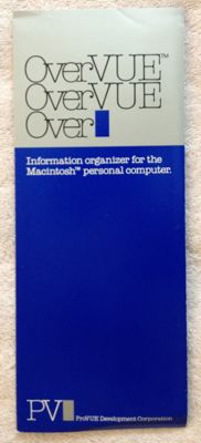
I was perusing an online catalog of old Apple memorabilia for sale (just looking), and was surprised to see that apparently someone thinks an old OverVUE is worth $50! I still have some of those flyers stashed away, apparently they are a potential gold mine
The catalog says this flyer is from 1988, but really that is probably 1985, or maybe even 1984. The caption is “2-color flyer from the excellent spreasheet-like database software”.
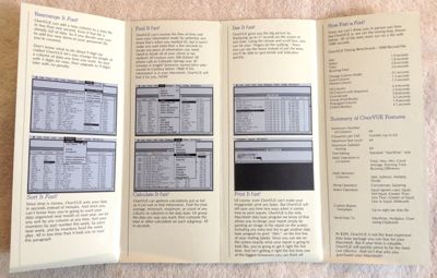
Sure, I’ve got manuals, boxes, complete packaging! I guess I can stop working on new software and retire on proceeds of memorabilia! Anyone wan’t a slightly used MacWorld Expo booth?
I have a working MacPlus (a whole extra MB of RAM!!!) and a massive 30MB external HD (which weighs about 5 kg), each of which cost me AU$1,000 in 1988. Sadly, I no longer have the dot-matrix printer which cost another $1,000. Look at what $3,000 buys you now!
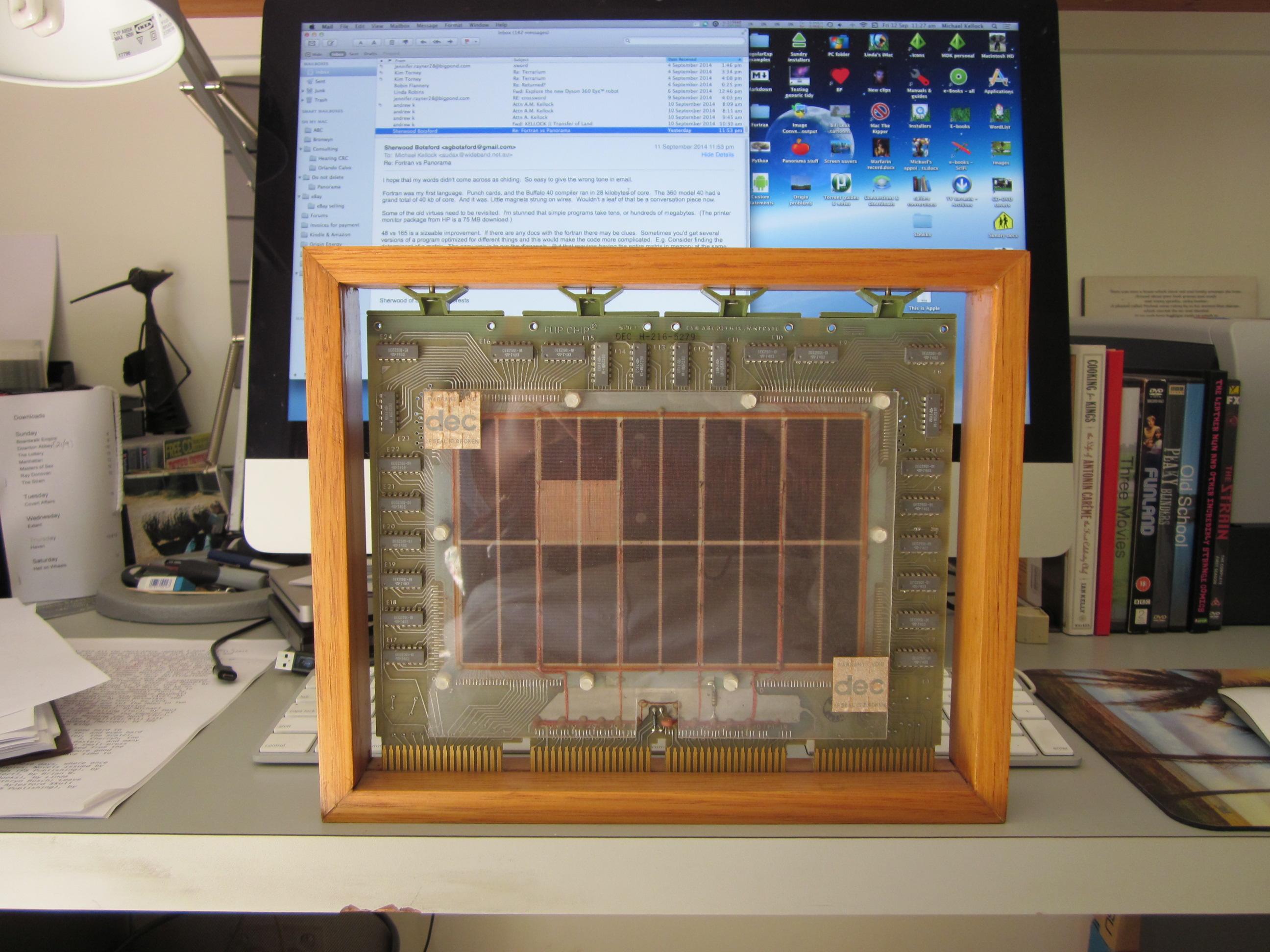
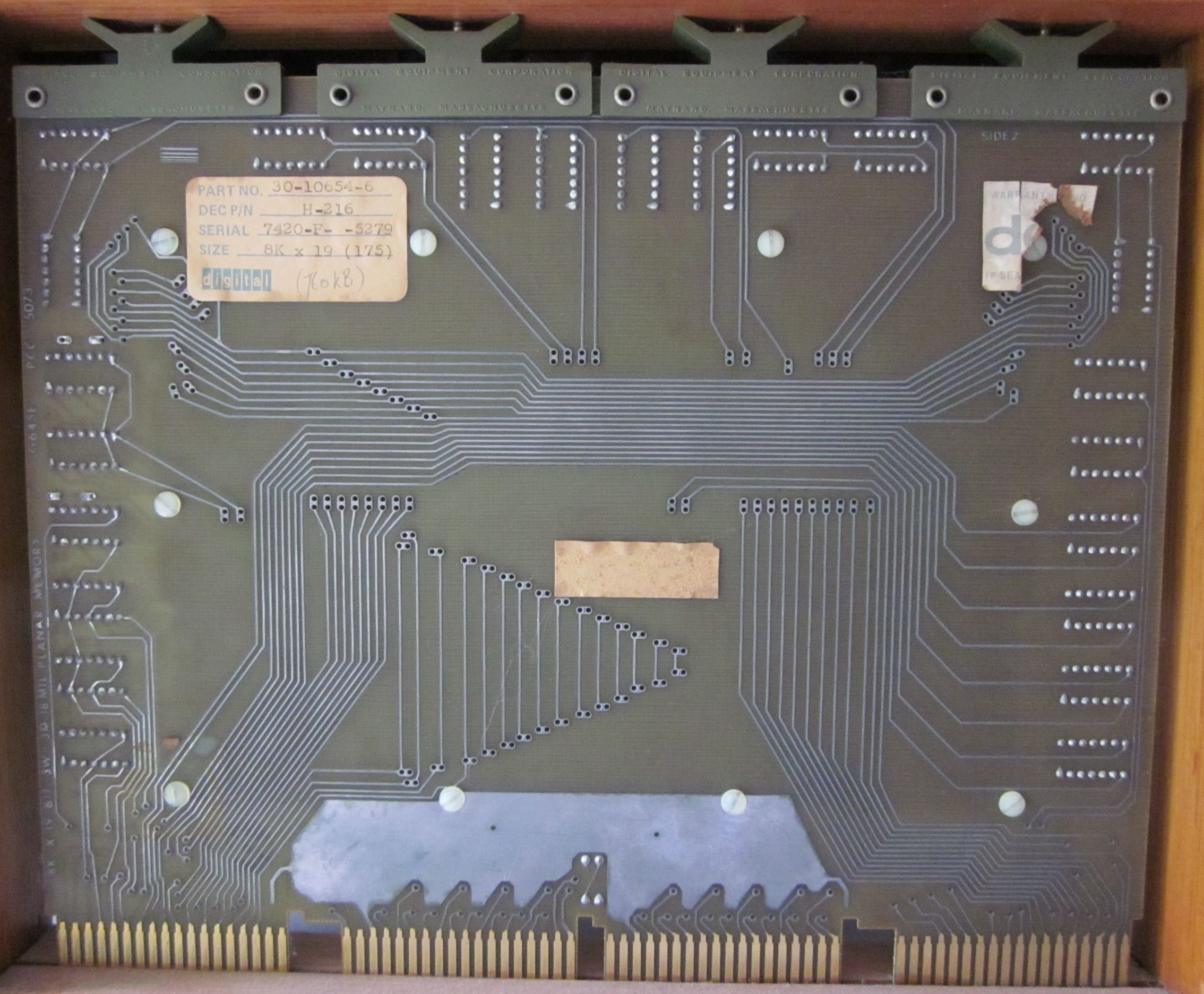
And here’s my DEC-10 memory board holding 19K 36-bit words - hand-wired in Singapore - they cost a king’s ransom back in the day:
Now that is really awesome! Could you by chance post a more close-up view of that board? I’ve never seen core memory that looked quite like that before. That looks like TTL logic around the edges, though I can’t read the part numbers.
You don’t here about DEC-10’s much, the PDP-8, PDP-11, and VAX are more famous. But at an early point in my career I used a system that had a spinoff of the DEC-10 operating system.
For those of you that get a chance to visit the San Jose area, the Computer History museum is really excellent. It’s right down the road from Google headquarters. If possible, you’ll want to spend several hours there (at least I did).
These are relatively low-res so I don’t overload your server - about 500 KB each. The originals are 1.4 MB if you want better or I can focus more closely on a particular section. Just in case anybody was wondering, the boards did not originally come in timber frames - I did that for safety and display purposes.
You can read the tag on the back - it says ‘8K x 19 (175)’. I know there are 19 panels (for want of a better word) but I’m not sure what the 8K or (175) refer to. My recollection of 19,000 36-bit words may be wrong.
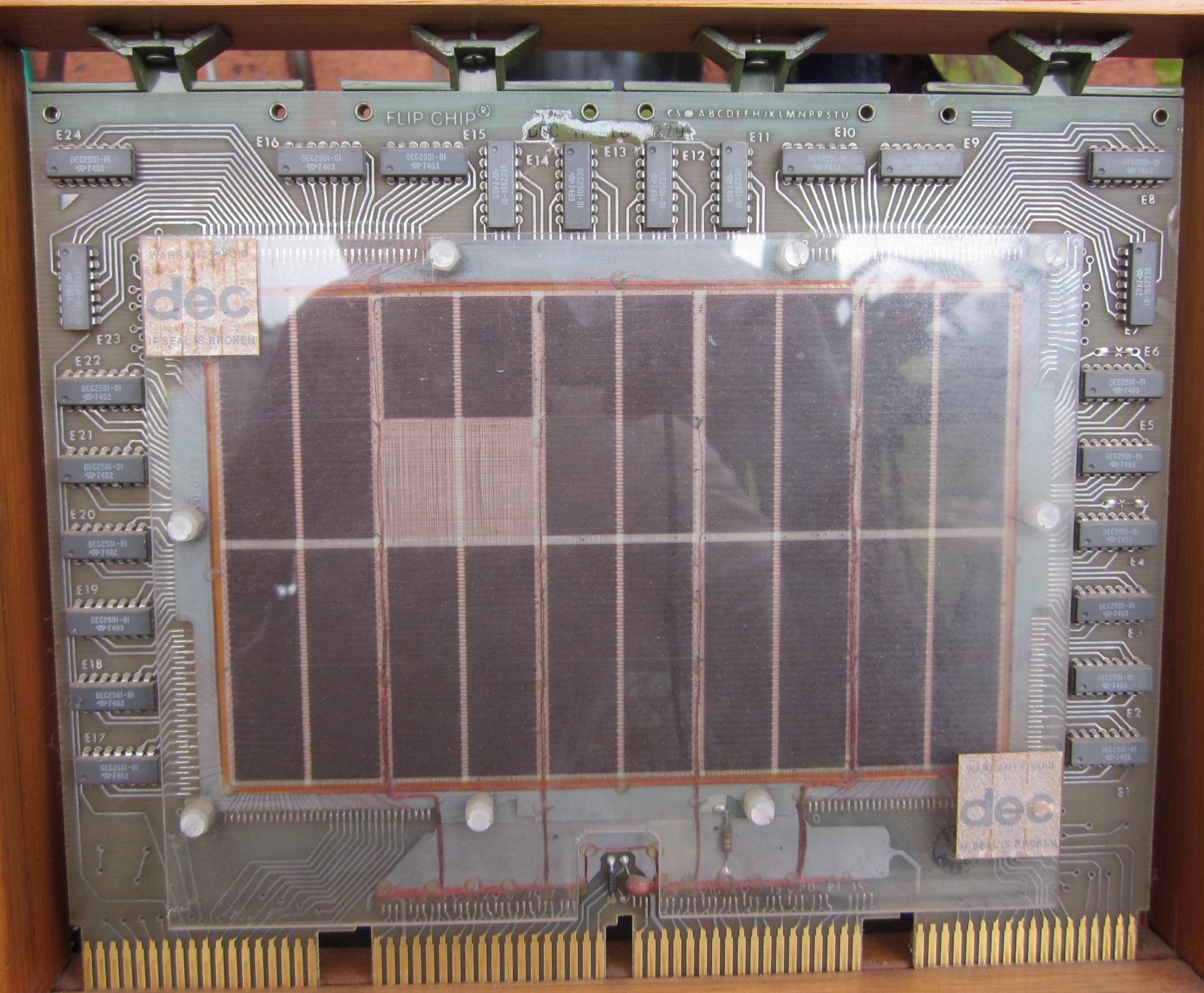
Yep, that’s 74XX TTL logic around the edges. Looks like mostly 7402 and 7403 chips, which are simple quad NOR and NAND gates. In other words, only 4 gates to a package, compared to billions in today’s chips!
I’m sure it’s not 19K words – memory is always going to come in a power of 2. I think 8K x 19 means 8192 words of 19 bits each – probably 18 data bits and one parity bit. With two boards that could give you 36 bit words. I’m so glad the computer industry has since standardized on 8 bit bytes – what a mess it was with the different word lengths of early machines! Maybe the 175 refers to the access time of the memory, perhaps 175ns? That’s kind of a guess on my part, but I can’t think of what else it could be.
I can’t quite tell – is the core memory itself mounted on a separate clear panel above the PC board? It looks like it might be ~10mm above the main board, supported by posts around the edges?
Could you email me the full size photos? I’d love to get an even closer look. Very cool that you kept this.
I wonder what “hand wired in Singapore” means. The core memory itself certainly looks much too dense to be hand wired, though I know earlier versions of core memory were hand wired (but much less densely. The PC board looks wave soldered. But maybe the connections between the PC board and the daughter board are done by hand.
No, that’s a perspex cover mounted on posts - presumably to keep sticky fingers off the wiring. And yes, the chips are 18 @ 7403 and 6 @ 7402.
I’m sure you’re correct in suggesting that the wiring is not hand-done, although that’s what I was told 45 years ago when I encountered my first DEC 10 as a masters student at the University of Queensland. DEC 10s were ubiquitous in Australian universities and were common in stock exchanges and other venues where time-sharing was needed. Lots of US universities also ran them.
I’ll get Linda to take some close-ups for you with her iPhone which does a much better job than my old Canon digital which is now a dinosaur. And I’ll send you the big photos.
Thanks for the closeup photos. That is so cool. In the closeups it definitely looks like the connections between the core array and the PC board are hand wired. Wow that must have been painstaking, it’s amazing this ever worked at all. And all of the wires are the same color! Look at the bundles running up the middle of the core array, you’d think there would be RF interference between the wires. Must have run at a fairly low frequency. And many of the wires run straight from the array to pins on the edge. Perhaps there was additional control logic on some other board.
How far we’ve come in a relatively short timeframe.
I could never understand why all those wires didn’t interfere with each other but, what the heck - it worked.
The other thing I was told about the hand wiring was that most of it was done by children because their hands were so much smaller - we’re talking about 40 years ago in what was then a third-worlds country, so maybe. I’d be interested to know how much of that is true and how much is/was urban myth.
Please send me the HiRes pics. I worked for a company 40 years ago that made memory with ferrite cores that were interweaved in a crosshatch pattern like a pot holder. I’m guessing that that is what we have here. The wires were strung from edge to edge on a rectangular frame.
We also made hard drives where the ‘head’ assembly moved in and out from the platter on an assembly with ball bearings on a ‘hopefully’ flat metal rail. There were multiple heads fixed like fingers that went in and out of the platter pack. (My job was purchasing all the components that made up the hard drives.) They had HEPA filters to ensure the minimal amount of air circulating around the inside the drive was clean. The hard drive cabinets were about the size of portable washing machines.
The DEC 10 had removable discs which were about 500 mm in diameter, weighed 5 kg or more and held, in today’s terms, a minuscule amount of data. And they also were loaded into washing machines.
Jim, might want to send them in (sell them) a little at a time so the market isn’t quickly diluted. All I saw was “paper”, no hardware. I have a perfectly good PB-180 with Math Co-Processor. Might be hard to find another battery but I’m pretty sure it boots up with the AC power cable.
Of course I have a bag-o-SCSI cables and analog modem.
Maybe I’ll boot it up and run some of my ZBasic programs.
I’m not planning on selling anything, I was just kidding about the gold mine part. My goal is to sell new modern software – not memorabilia
I sent a letter off to the owner of the web site, and it turns out he was delighted to hear from me since OverVUE was his favorite program at that time!